Our core competencies lie in the implementation of research and development projects in the fields of analytics and quality assurance (QA) with a focus on: New materials, electronic devices, thin and ultra-thin films, surfaces, and micro- and nanostructures.
Research Areas
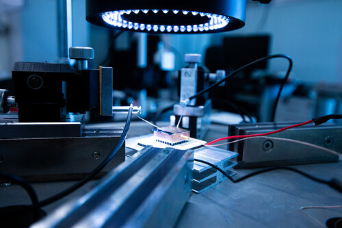
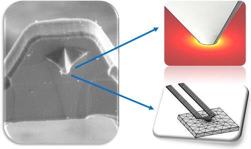
Thermal characterisation of thin films
- Measurement methods: 3-omega method, scanning thermal microscopy (SThM), infrared camera
- Measurement of thermal conductivities and thermal contact resistances
- Qualitative comparison of directly adjacent layers with regard to thermal conductivity
- Materials: SiO2, BN, AlN, MgO etc.
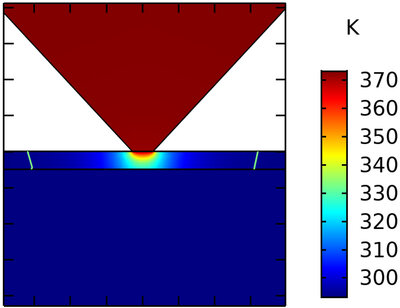
Thermal simulations
- Programmes: COMSOL Multiphysics for FEM simulations, MATLAB
- Simulation of heat propagation in (ultra)thin films
- Further development of thermal measurement methods
- Simulation of microelectronic structures
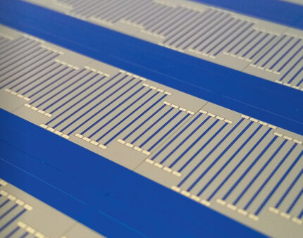
Electrical characterisation of thin films
- Measurement methods: Conductive Atomic Force Microscopy (C-AFM), Peakforce TUNA, Scanning Capacitance Microscopy (SCM) and Kelvin Probe Force Microscopy (KPFM), Van der Pauw method
- Spatially resolved determination of qualitative electrical conductivity by current maps
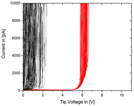
- I-V spectroscopy, e.g. to determine the breakdown voltage
- Measurement of surface potentials and local dopant variations
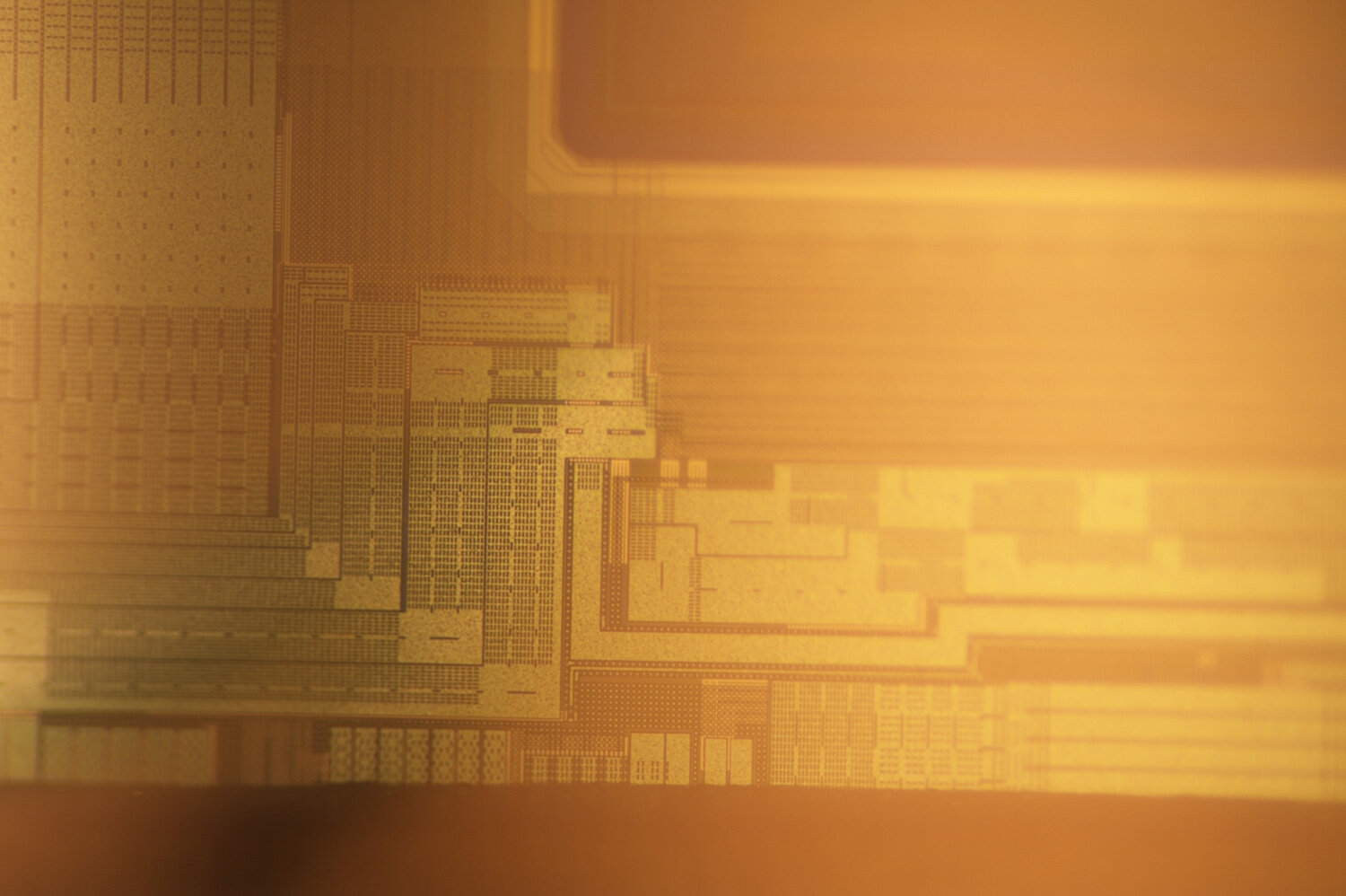
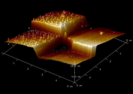
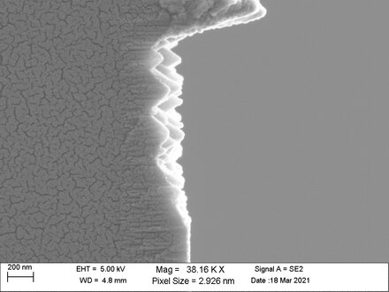
Structural and topographical investigations
- Measurement methods: AFM, SEM, LSM
- Investigation of thin layers with regard to material composition, impurities, surface structures, roughness, etc.
- Creation of 3-dimensional surface profiles
- Measurement of micro- and nanostructures
Reliability analyses
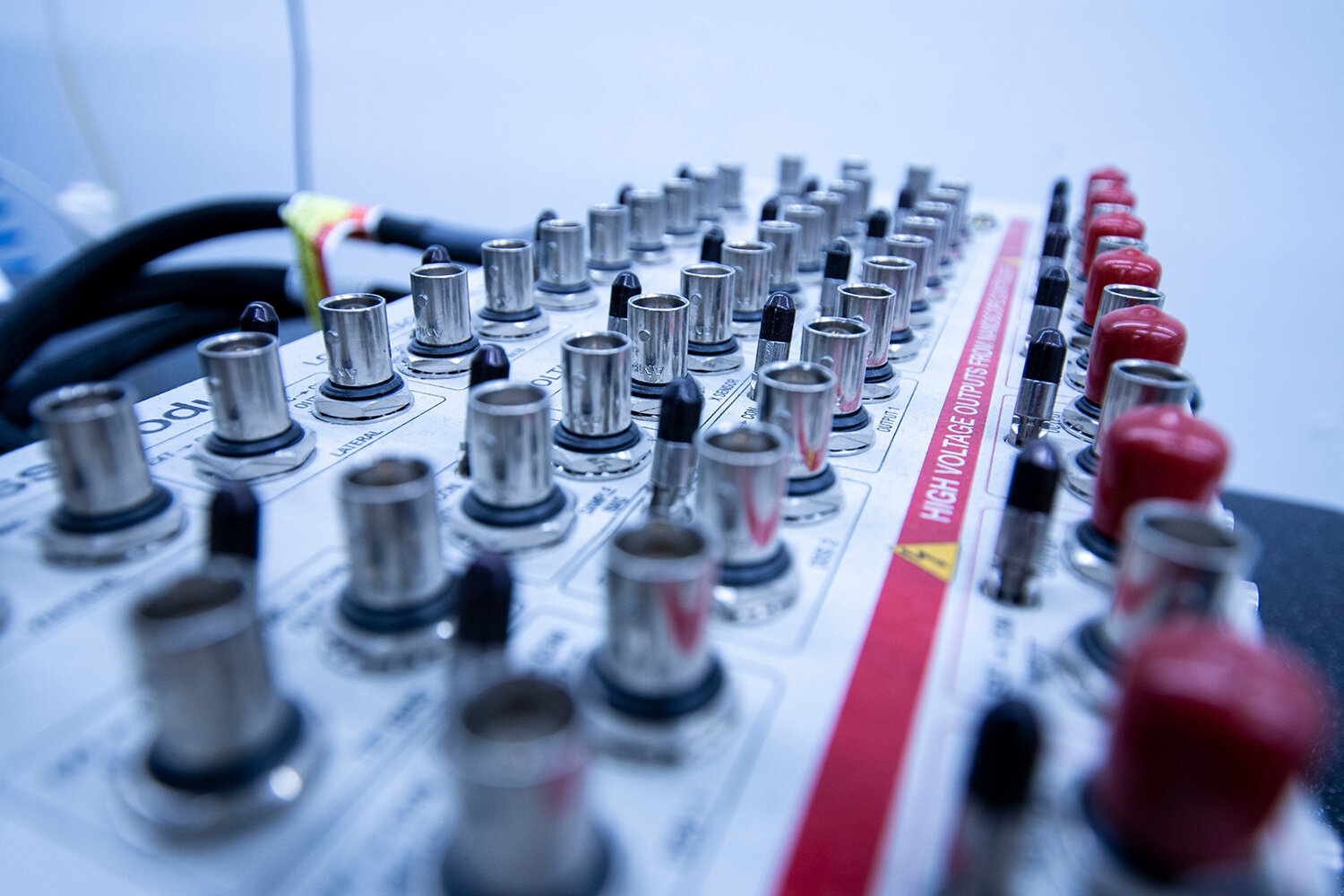
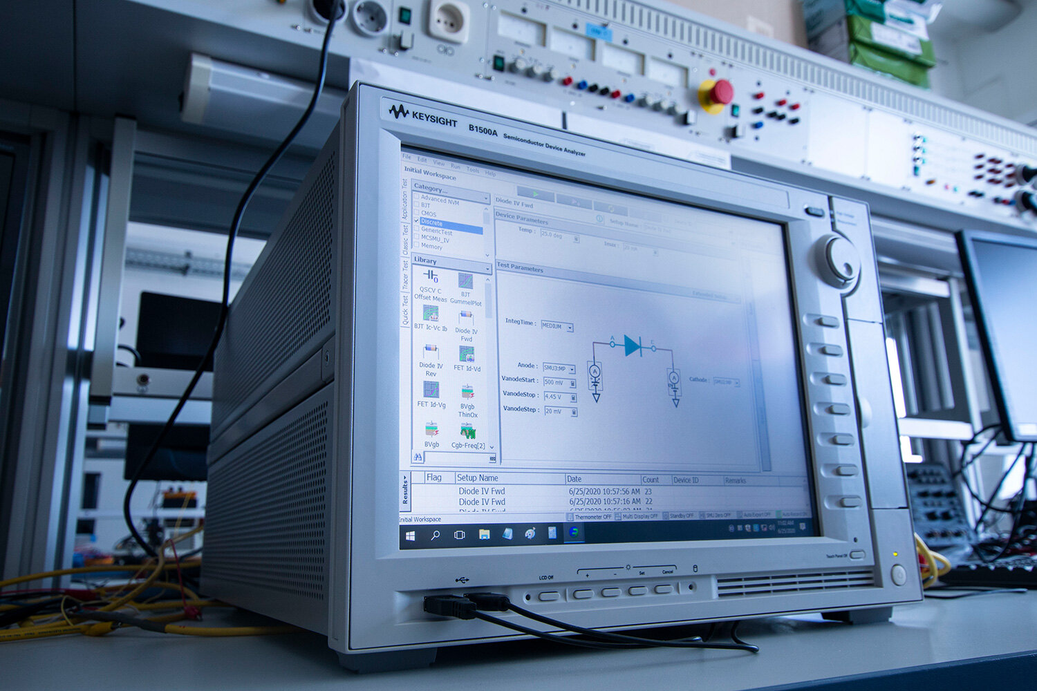
- Measurement methods: Keysight B1500 Semiconductor Parameter Analyser, Cascade 12k Summit Prober, Süss PA300 Probestation
- TDDB tests: Constant Voltage Stress (CVS), Ramped Voltage Stress (RVS), Constant Current Stress (CCS) and Temperature Stress from -50 to 200 °C
- Extrapolation of the lifetime of electronic components based on various physical models
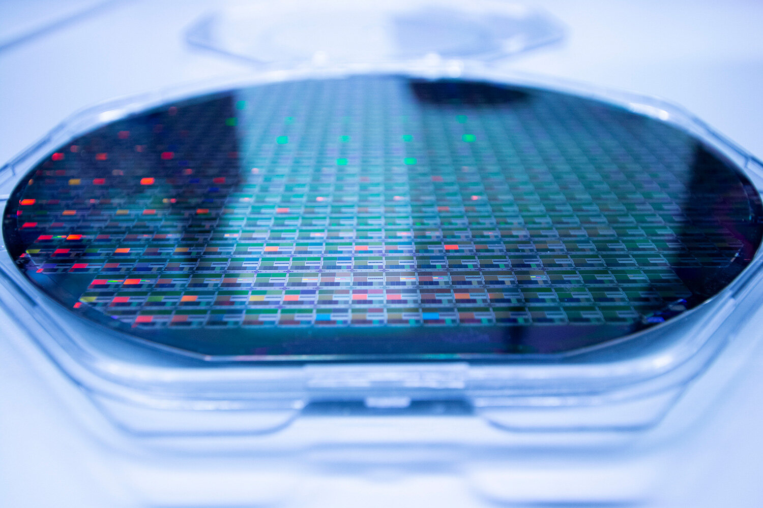
- Wafer level testing up to 300 mm

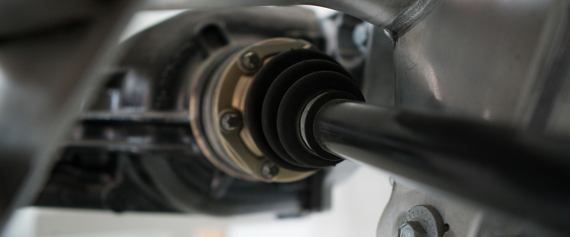
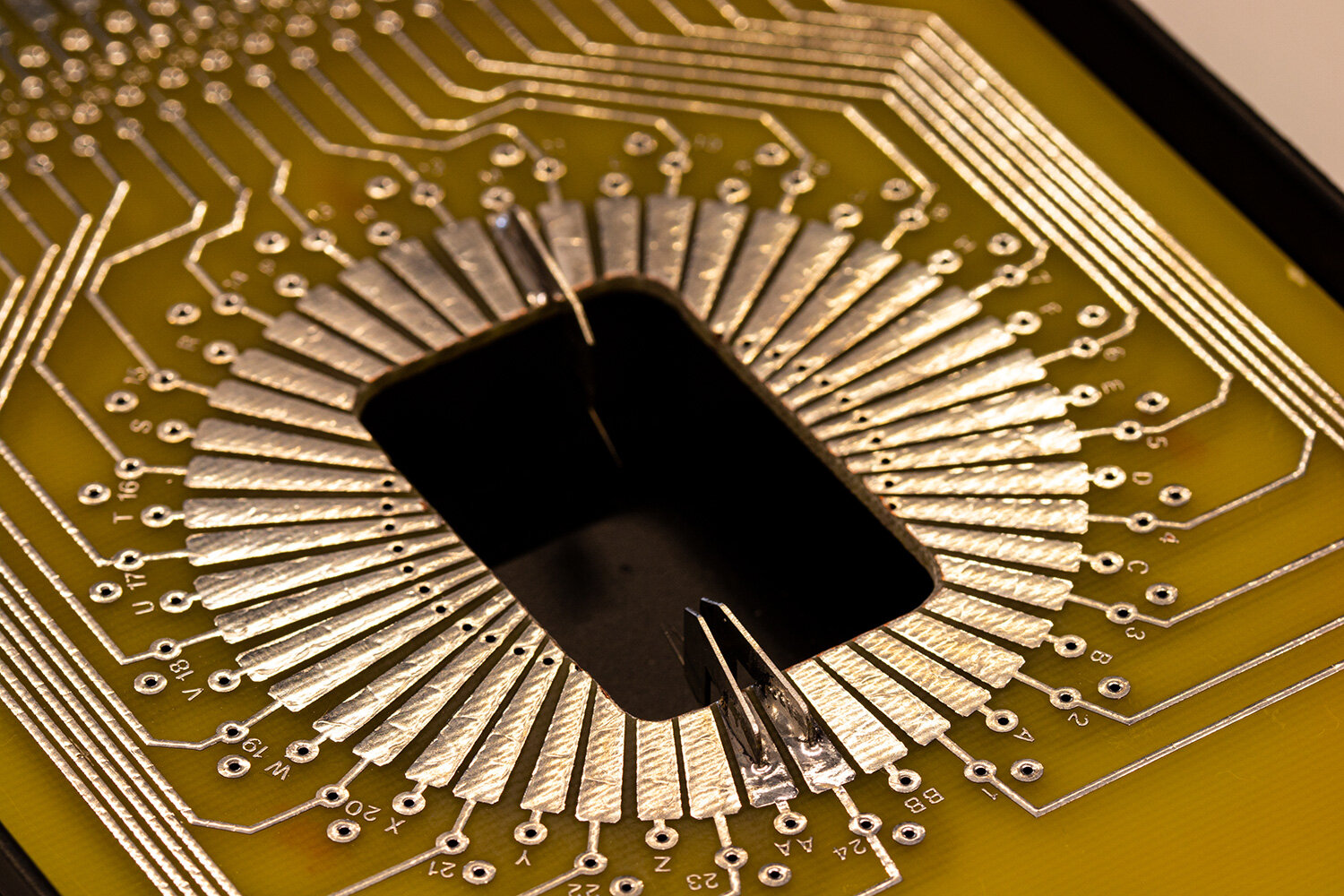
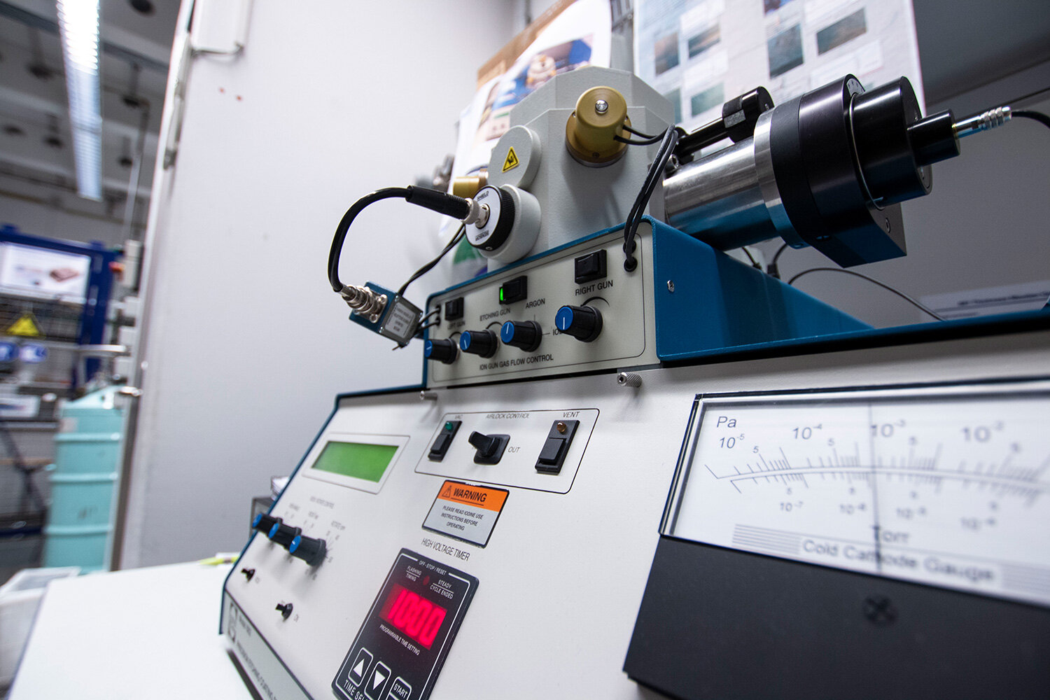
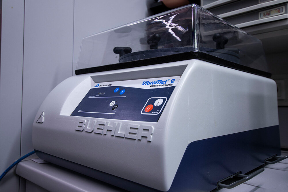
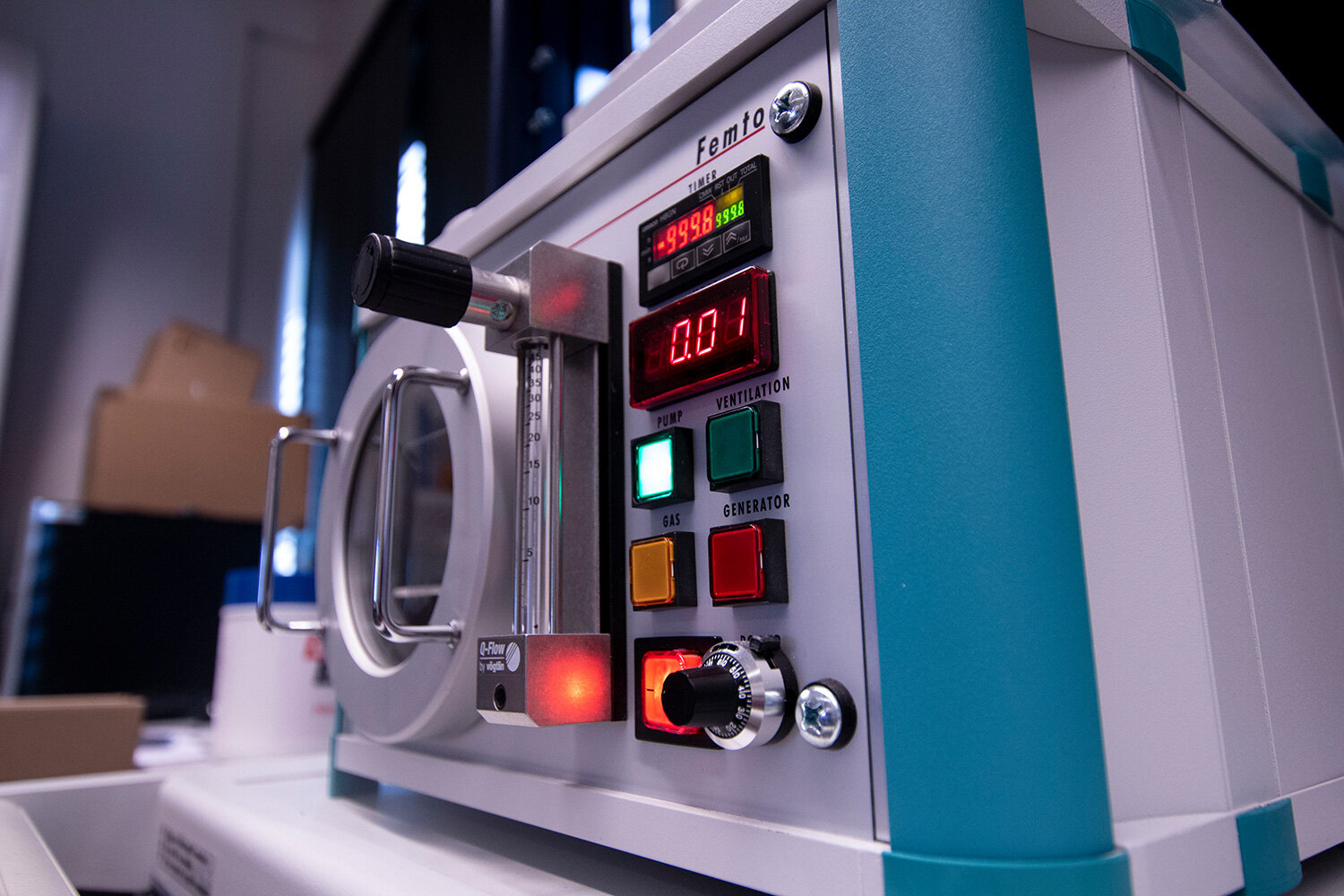
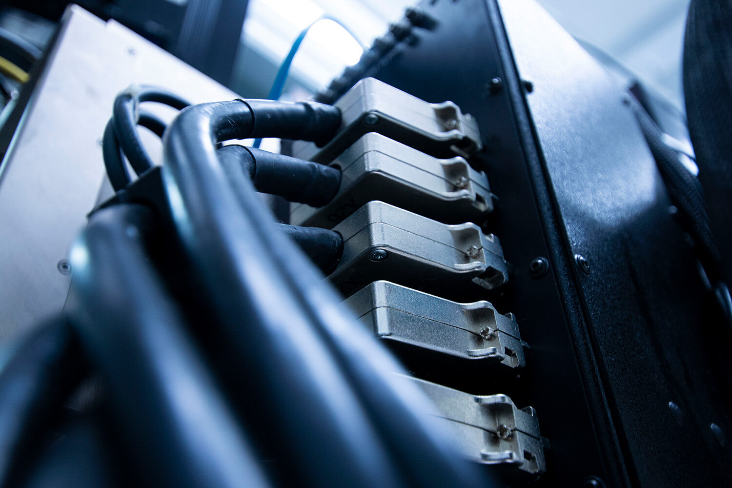
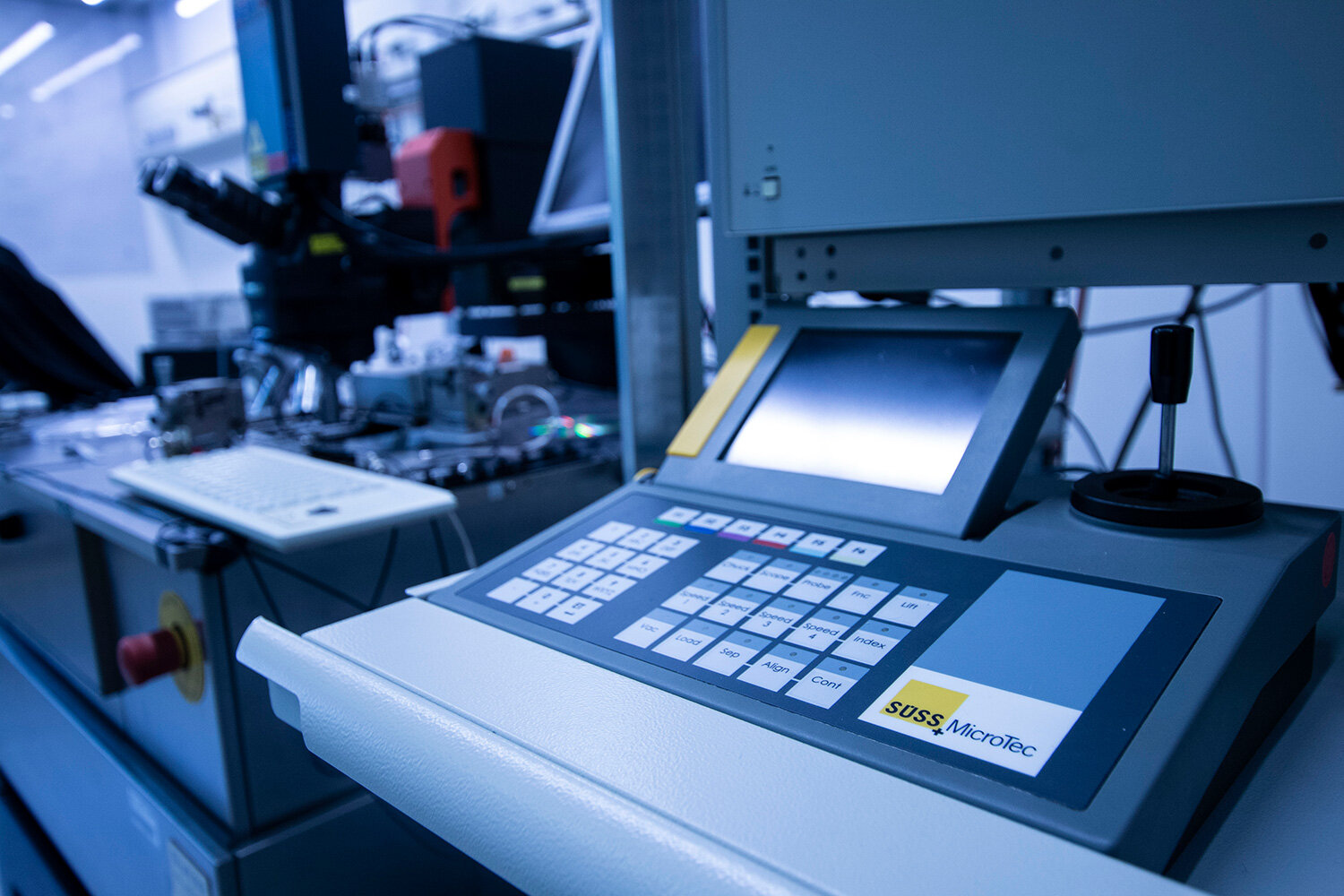
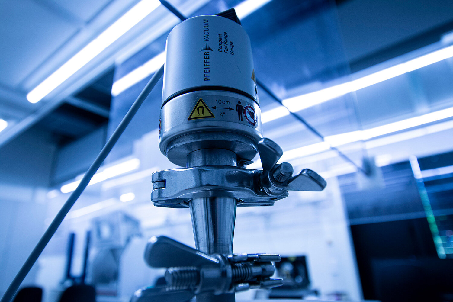
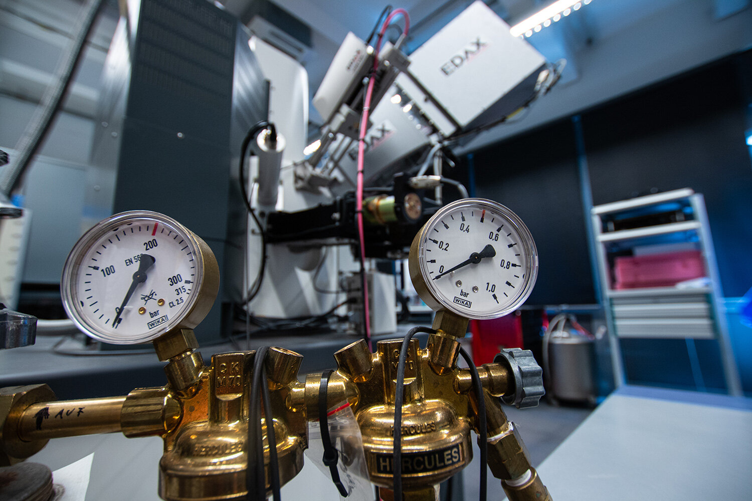
Lab Equipment
|
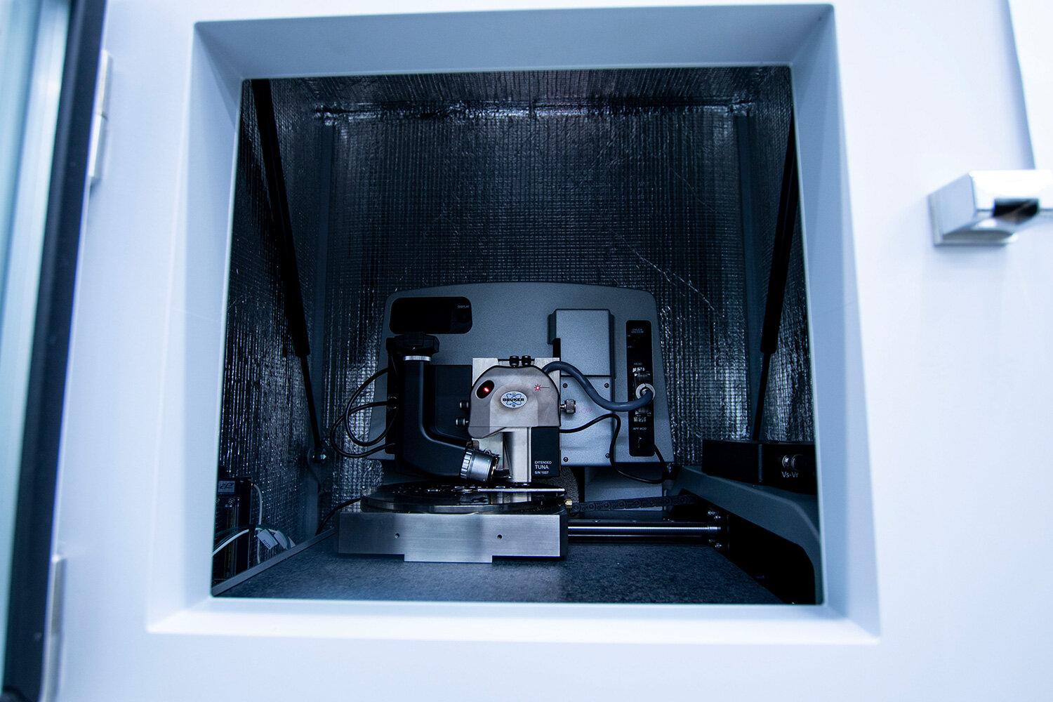
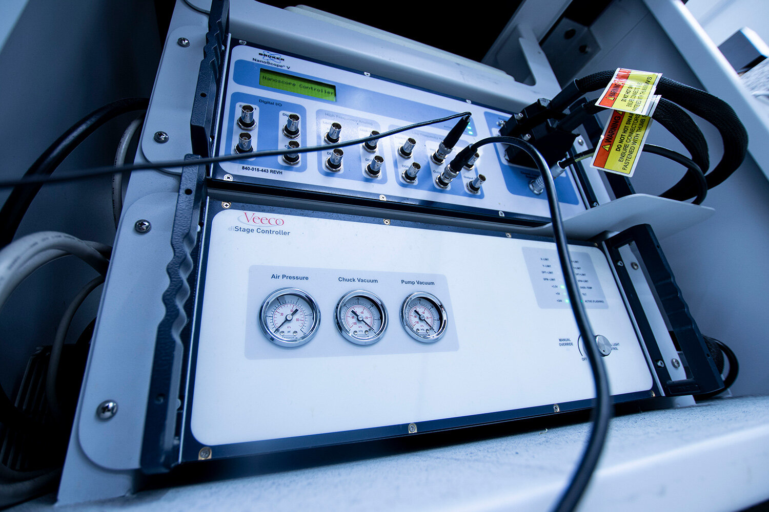
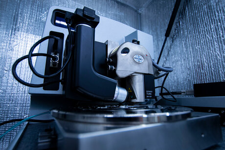
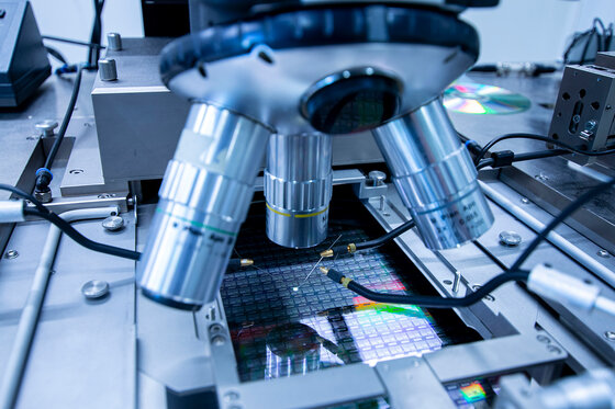
Scanning Probe Microscopy (AFM)
|
|
|
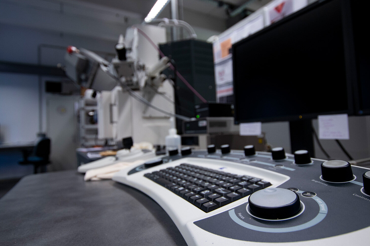
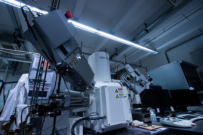
Scanning Electron Microscopy (SEM) & STEM
|
|
|
3-Omega Methodology
|
|
|
Infrared camera
|
|
|
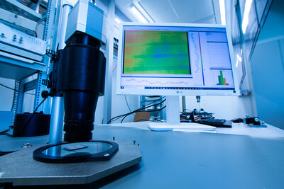
Laser scanning microscopy
|
|
|
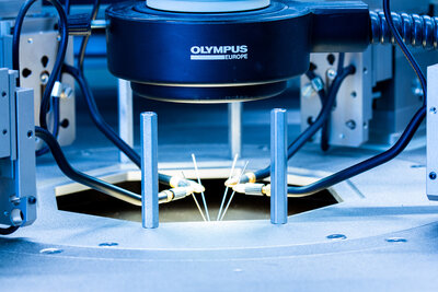
Wafer prober
|
|
|
Van der Pauw methodology
|
 |


Publications
You can find all publications of the IQMA in our publications database.
Below you will find a selection of relevant journal articles, book contributions and patents of the working group.
Metzke, C., Kühnel, F., Weber, J., & Benstetter, G. (2021). Scanning Thermal Microscopy of Ultrathin Films: Numerical Studies Regarding Cantilever Displacement, Thermal Contact Areas, Heat Fluxes, and Heat Distribution. Nanomaterials, 11(2), 491.
https://doi.org/10.3390/nano11020491
Ni, W., Niu, C., Zhang, Y., Liu, L., Cui, Y., Fan, H., ... & Lei, G. (2021). Modeling W fuzz growth over polycrystalline W due to He ion irradiations at an elevated temperature. Journal of Nuclear Materials, 550, 152917.
https://doi.org/10.1016/j.jnucmat.2021.152917
Wen, C., Banshchikov, A. G., Illarionov, Y. Y., Frammelsberger, W., Knobloch, T., Hui, F., ... & Lanza, M. (2020). Dielectric Properties of Ultrathin CaF2 Ionic Crystals. Advanced Materials, 32(34), 2002525.
https://doi.org/10.1002/adma.202002525
Fan, H., Zhang, Y., Liu, D., Niu, C., Liu, L., Ni, W., ... & Lei, G. (2020). Tensile stress-driven cracking of W fuzz over W crystal under fusion-relevant He ion irradiations. Nuclear Fusion, 60(4), 046011.
https://doi.org/10.1088/1741-4326/ab71bb
Metzke, C., Frammelsberger, W., Weber, J., Kühnel, F., Zhu, K., Lanza, M., & Benstetter, G. (2020). On the limits of scanning thermal microscopy of ultrathin films. Materials, 13(3), 518.
https://doi.org/10.3390/ma13030518
Wen, C., Jing, X., Hitzel, F. F., Pan, C., Benstetter, G., & Lanza, M. (2019). In situ observation of current generation in ZnO nanowire based nanogenerators using a CAFM integrated into an SEM. ACS applied materials & interfaces, 11(17), 15183-15188.
https://doi.org/10.1021/acsami.9b00447
Bi, Z., Liu, D., Zhang, Y., Liu, L., Xia, Y., Hong, Y., ... & Yan, L. (2019). The evolution of He nanobubbles in tungsten under fusion-relevant He ion irradiation conditions. Nuclear Fusion, 59(8), 086025.
https://doi.org/10.1088/1741-4326/ab2472
Jiang, L., Weber, J., Puglisi, F. M., Pavan, P., Larcher, L., Frammelsberger, W., ... & Lanza, M. (2019). Understanding current instabilities in conductive atomic force microscopy. Materials, 12(3), 459.
https://doi.org/10.3390/ma12030459
Chen, S., Jiang, L., Buckwell, M., Jing, X., Ji, Y., Grustan‐Gutierrez, E., ... & Lanza, M. (2018). On the limits of scalpel AFM for the 3D electrical characterization of nanomaterials. Advanced Functional Materials, 28(52), 1802266.
https://doi.org/10.1002/adfm.201802266
Yang, C., Souchay, D., Kneiß, M., Bogner, M., Wei, H. M., Lorenz, M., ... & Grundmann, M. (2017). Transparent flexible thermoelectric material based on non-toxic earth-abundant p-type copper iodide thin film. Nature communications, 8(1), 1-7.
https://doi.org/10.1038/ncomms16076
Jing, X., Panholzer, E., Song, X., Grustan-Gutierrez, E., Hui, F., Shi, Y., ... & Lanza, M. (2016). Fabrication of scalable and ultra low power photodetectors with high light/dark current ratios using polycrystalline monolayer MoS2 sheets. Nano Energy, 30, 494-502.
https://doi.org/10.1016/j.nanoen.2016.10.032
Fan, H., You, Y., Ni, W., Yang, Q., Liu, L., Benstetter, G., ... & Liu, C. (2016). Surface degeneration of W crystal irradiated with low-energy hydrogen ions. Scientific reports, 6(1), 1-9.
https://doi.org/10.1038/srep23738
Liu, L., Liu, D., Hong, Y., Fan, H., Ni, W., Yang, Q., ... & Li, S. (2016). High-flux He+ irradiation effects on surface damages of tungsten under ITER relevant conditions. Journal of Nuclear Materials, 471, 1-7.
https://doi.org/10.1016/j.jnucmat.2016.01.001
Hamann, L., Benstetter, G., Hofer, A., Mattheis, J., Haas, M., & Zapf-Gottwick, R. (2015). Use of Coated-Metal Particles in Rear Busbar Pastes to Reduce Silver Consumption. IEEE Journal of Photovoltaics, 5(2), 534-537.
https://doi.org/10.1109/JPHOTOV.2014.2388080
Yang, Q., You, Y. W., Liu, L., Fan, H., Ni, W., Liu, D., ... & Wang, Y. (2015). Nanostructured fuzz growth on tungsten under low-energy and high-flux He irradiation. Scientific reports, 5(1), 1-9.
https://doi.org/10.1038/srep10959
Berthold, T., Benstetter, G., Frammelsberger, W., Rodríguez, R., & Nafría, M. (2015). Nanoscale characterization of CH3-terminated Self-Assembled Monolayer on copper by advanced scanning probe microscopy techniques. Applied Surface Science, 356, 921-926.
https://doi.org/10.1016/j.apsusc.2015.08.182
Yang, Q., Fan, H., Ni, W., Liu, L., Berthold, T., Benstetter, G., ... & Wang, Y. (2015). Observation of interstitial loops in He+ irradiated W by conductive atomic force microscopy. Acta Materialia, 92, 178-188.
https://doi.org/10.1016/j.actamat.2015.04.004
Iglesias, V., Lanza, M., Zhang, K., Bayerl, A., Porti, M., Nafría, M., ... & Bersuker, G. (2011). Degradation of polycrystalline HfO2-based gate dielectrics under nanoscale electrical stress. Applied physics letters, 99(10), 103510.
https://doi.org/10.1063/1.3637633
Benstetter, G., Biberger, R., & Liu, D. (2009). A review of advanced scanning probe microscope analysis of functional films and semiconductor devices. Thin Solid Films, 517(17), 5100-5105.
https://doi.org/10.1016/j.tsf.2009.03.176
G. Benstetter, P. Breitschopf, B. Knoll - US Patent 7,788,732, 2010
Frammelsberger, W., Benstetter, G., Kiely, J., & Stamp, R. (2007). C-AFM-based thickness determination of thin and ultra-thin SiO2 films by use of different conductive-coated probe tips. Applied Surface Science, 253(7), 3615-3626.
https://doi.org/10.1016/j.apsusc.2006.07.070
Frammelsberger, W., Benstetter, G., Kiely, J., & Stamp, R. (2006). Thickness determination of thin and ultra-thin SiO2 films by C-AFM IV-spectroscopy. Applied Surface Science, 252(6), 2375-2388.
https://doi.org/10.1016/j.apsusc.2005.04.010
Lanza, M., (Ed.). (2017). Conductive Atomic Force Microscopy: Applications in Nanomaterials. John Wiley & Sons
ISBN: 978-3-527-34091-0
projects
Current Projects:
Finished Projects:
Current Student Projects
We regularly offer exciting topics in the areas of electrical and thermal material characterisation, as well as analytics and reliability topics for modern electronic components. Interested students from the fields of applied computer science, mechatronics, electrical engineering, media technology and technical physics can work on these topics in the form of bachelor's theses and master's theses, possibly also with industry participation, Master of Applied Research topics and SHK positions. For detailed information, please see the following PDF.
Contact & Directions
The following professors and (research) assistants work at the IQMA. For enquiries, please contact Prof Benstetter.

Buildings E and L at the campus in Deggendorf.
You can find the offices of the staff members under the respective staff link.
Laboratories:
- Room E108: Electronic Devices (in german)
- Rooms E007 and L005: Scanning electron microscopy (SEM) and semiconductor analysis (in german)
- Rooms E015 and L006: Scanning Probe Microscopy (RSM) (in german)