Zentrum für angewandte Forschung
Technologie Campus Teisnach Sensorik I 4.0
Wissenschaftlicher Mitarbeiter
TCTS O 17
09923/80108-506
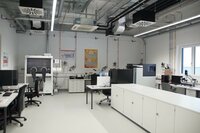
Material- und Oberflächenanalytik
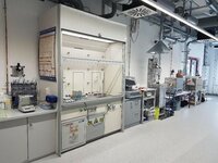
TC Teisnach
Material- und Schichttechnik